

NAND and NOR Implementation
Digital circuits are more frequently constructed with NAND or NOR gates than with AND and OR gates. NAND and NOR gates are easier to fabricate with electronic components and are the basic gates used in all IC digital logic families. The procedure for two-level implementation is presented in this section.
NAND and NOR conversions (from AND, OR and NOT implemented Boolean functions)
Because of the prominence of NAND and NOR gates in the design of digital circuits, rules and procedures have been developed for the conversion from Boolean functions given in terms of AND, OR, and NOT into equivalent NAND and NOR logic diagrams.
To facilitate the conversion to NAND and NOR logic, there are two other graphic symbols for these gates.
NAND implementation
The implementation of a Boolean function with NAND gates requires that the function be simplified in
the sum of products form. To see the relationship between a sum of products expression and its
equivalent NAND implementation, consider the logic diagrams of Fig below. All three diagrams are
equivalent and implement the function: F=AB + CD + E
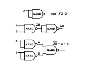
The rule for obtaining the NAND logic diagram from a Boolean function is as follows:
First method:
(a) Simplify the function and express it in the sum of products.
(b) Draw a NAND gate for each product term of the function that has at least two literals. The inputs to each NAND gate are the literals of the term. This constitutes a group of first-level gates.
(c) Draw a single NAND gate (using the AND-invert or invert-OR graphic symbol) in the second level, with inputs coming from outputs of first-level gates.
(d) A term with a single literal requires an inverter in the first level or maybe complemented and applied as an input to the second-level NAND gate.
Second method:
If we combine the 0’s in a map, we obtain the simplified expression of the complement of the function in sum of products. The complement of the function can then be implemented with two levels of NAND gates using the rules stated above. If the normal output is desired, it would be necessary to insert a one input NAND or inverter gate. There are occasions where the designer may want to generate the complement of the function; so this second method may be preferable.
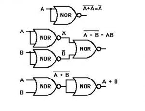
NOR Implementation
The NOR function is the dual of the NAND function. For this reason, all procedures and rules for NOR logic are the duals of the corresponding procedures and rules developed for NAND logic. The implementation of a Boolean function with NOR gates requires that the function be simplified in a product of sums form. A product of sums expression specifies a group of OR gates for the sum terms, followed
by an AND gate to produce the product. The transformation from the OR-AND to the NOR-NOR diagram is depicted in Fig below. It is similar to the NAND transformation discussed previously, except that now we use the product of sums expression.
You may also like Karnaugh Map
Leave a Reply