
")
Introduction
The Data flipflop is designed to overcome the problem of forbidden states and rest condition. It has single inputs that are inverted using NAND gates. The single input is called ‘D’ input. The ‘D’ flipflop is the modification of clock S-R flipflop.
In normal clock S-R flipflop, two separate inputs are required to SET and RESET the flipflop usually. This two-input are generated by two separate combinational circuits and may not be produced simultaneously. These may give rise to undesired output which may be a disadvantage in certain activation.
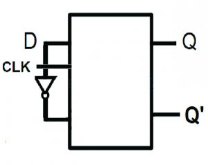
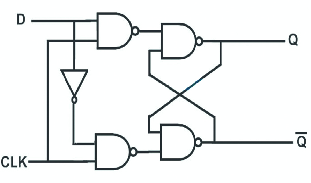
The Logic Circuit Of Data flipflop
Truth Table For D-flipflop
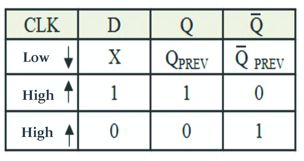
Simply, for positive transition on clock signal,
If D = 0 => Q = 0 so flip flop is reset.
If D = 1 => Q = 1 so flip flop is set.
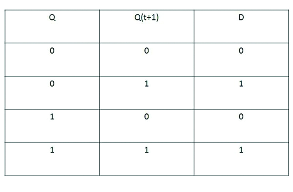
Characteristics Equation For D-flipflop
Q(t+1) = T'(t)Q(t) + T(t)Q'(t) = T(t) ⊕ Q(t)
Excitation Table
Therefore, this is the short explanation of D-Flipflop.
You may also like :Seven Segment Display
Leave a Reply