

Combinational Circuit
Combinational Circuit consists of logic gates whose output at any instant of time are determined by the present combination of input. Basic building blocks of a combination of the logic circuit.
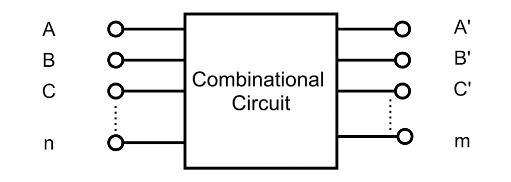
Fig: Combinational Circuit
There is ‘n’ numbers of inputs line and “m” numbers of the output lines. for “n” inputs. There is 2n possible combination of binary values for each possible input combination.
It can be discovered by M Boolean function of each output variable.
Design procedure
The designed circuit starts from the verbal combination and verbal outline and ends with a logic circuit diagram.
The procedure includes in the following steps:-
1. Specification
Write a specification for the circuit if one is not already available
2. Formulation
Derive a truth table or initial Boolean equations that define the required relationships between the inputs and outputs, if not in the specification.
Apply hierarchical design if appropriate
3. Optimization
Apply 2-level and multiple-level optimization
Draw a logic diagram for the resulting circuit using ANDs, ORs, and inverters
4. Technology Mapping
Map the logic diagram to the implementation technology selected
5. Verification
Verify the correctness of the final design manually or using simulation
In simple words, we can list out the design procedure of combinational circuits as:
- State the given problem completely and exactly.
- Interpret the problem and determine the available input variable and require the output variable.
- Assign a latter symbol to each input and output variable.
- Design the truth table which defines the required relation between outputs and inputs.
- Obtain the simplified Boolean expression for each output.
- Draw the Logic diagram to implement the Boolean expression.
Leave a Reply