

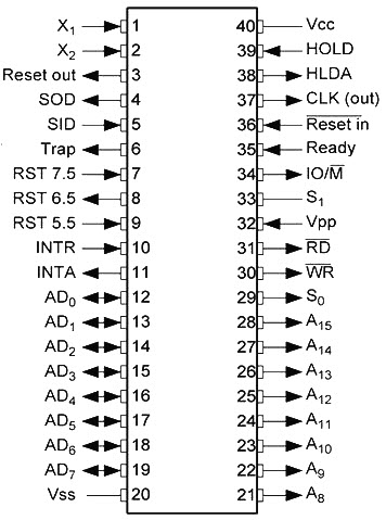
Pin Diagram of 8085 Microprocessor
The 8085 microprocessor is an 8-bit general-purpose processor that can deal with the memory of 64K Byte. This microprocessor consists of 40-pins as well as works with a +5V power supply. This processor can be work at a 3 MHz of maximum frequency.
This processor is available in three versions such as 8085 AH, 8085 AH1, and 8085 AH2 which are designed with HMOS technology. The highly developed versions use 20% of the power supply. The 40 pins of the microprocessor can be divided into six groups such as address bus, data bus, control signals & status signals; power supply & frequency, externally started signals and serial input/output ports.
- It has 40 pins and uses +5V for power.
- It is an 8-bit microprocessor.
- It is an appended version of the 8080 microprocessor.
- It can run at a maximum frequency of 3 MHz.
- The maximum memory attached to the 8085 microprocessor is 64 KB.
The pins on the chip can be grouped into 6 groups:
- Power supply and frequency
- Serial I/O ports
- Address Bus
- Data Bus
- Control and Status Signals
- Externally Initiated Signals
Power supply and Frequency signals
The microprocessor operates on a single +5V power supply connected to Vcc at pin number 40. The ground is connected to Vss at pin number 20. There are 3 pins in the frequency control group
- X0
- X1
- CLK OUT
Serial I/O ports
These signals are used for giving serial input and output data. There are two pins for serial I/O data i.e.
(i)SID: Serial Input Data (Pin number 5).
- This pin provides serial input data. The serial data on this pin is loaded into the seventh bit of the accumulator when RIM instruction is executed. RIM stands for reading INTERRUPT MASK, which checks whether the interrupt is masked or not.
(ii)SOD: Serial Out Data (Pin number 4).
- This pin provides the serial output data. The serial data on this pin delivers its output to the seventh bit of the accumulator when SIM instruction is executed.
Address Bus
- The address bus has 8 signal lines A8 – A15 which are unidirectional.
- The address bus also a set of parallel-connected lines.
- The address bus consists of 16, 20, 24 or 32 parallel lines.
- The address bus carries the address of the memory or I/O location to be read or written from.
- The address bus is available from pin number 21 to 28.
Data Bus
- The other 8 address bits are multiplexed (time-shared) with the 8 data bits.
- The bits AD0 – AD7 are bi-directional and serve as A0 – A7 and D0 – D7 at the same time.
- During the execution of the instruction, these lines carry the address bits during the early part, then during the late parts of the execution, they carry the 8 data bits.
- In order to separate the address from the data, we can use a latch to save the value before the function of the bits changes.
- The data bus consists of 8, 16 or 32 parallel lines. .The data bus is a bidirectional bus. The data bus can transfer the data from CPU to memory or vice versa. The data bus also connects the I/O ports and microprocessors.
- Pin numbers 12 to 19 are used for data buses in the microprocessor.
Control and Status Signals
There are 3 main control and status signals; RD, WR & ALE
ALE: Address Latch Enable
- This signal is a pulse that becomes high when the AD0 – AD7 lines have an address on them. It becomes 0 after that.
- This signal can be used to enable a latch to save the address bits from the AD lines.
- Pin number 30.
Externally Initiated Signals
These are asynchronous in nature. They are 4 signals and they are:
- RESET’
- READY’
- INTERRUPT
- DMA
You may also like Assembly language programming with 8085 microprocessor
Leave a Reply