

I/O and Memory Read/Write Timing Diagrams
In I/O and Memory Read/Write Timing Diagrams as a CPU need to communicate with the various memory and input-output devices (I/O) as we know data between the processor and these devices flow with the help of the system bus.
There are three ways in which system bus can be allotted to them :
- A separate set of address, control and data bus to I/O and memory.
- Have a common bus (data and address) for I/O and memory but separate control lines.
- Have a common bus (data, address, and control) for I/O and memory.
Several memory chips and I/O devices are connected to a microprocessor. The following figure shows a schematic diagram to interface memory chips and I/O devices to a microprocessor.
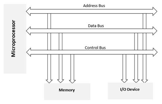
Memory Interfacing
When we are executing any instruction, the address of memory location or an I/O device is sent out by the microprocessor. The corresponding memory chip or I/O device is selected by a decoding circuit. Memory requires some signals to read from and write to registers and the microprocessor transmits some signals for reading or writing data.
The interfacing process includes matching the memory requirements with the microprocessor signals. Therefore, the interfacing circuit should be designed in such a way that it matches the memory signal requirements with the microprocessor’s signals.
I/O interfacing
As we know, keyboards and displays are used as communication channels with the outside world. Therefore, it is necessary that we interface the keyboard and display it with the microprocessor. This is called I/O interfacing.
For this type of interfacing, we use latches and buffers for interfacing the keyboards and displays with the microprocessor. But the main drawback of this interfacing is that the microprocessor can perform only one function and so on.
You may also like Execute Operation and Timing Diagram
Leave a Reply